Manabu Yoshida (Senior Researcher), Printed Electronics Device Team (Leader: Noriyuki Takada), the Flexible Electronics Research Center (Director: Toshihide Kamata) of the National Institute of Advanced Industrial Science and Technology (AIST; President: Tamotsu Nomakuchi), has developed a technique to form an aluminum or copper UHF-RFID antenna on a flexible substrate by printing, in collaboration with Taiyo Holdings Co., Ltd.
Taiyo Holdings has developed aluminum and copper pastes used in the pressure annealing technique developed by AIST. By applying the pressure annealing technique in the air to the metal pattern printed using the developed metal pastes, the surface of the pattern has become electroconductive. This technique can be easily incorporated into the conventional printing process and is expected to contribute to the widespread use of printed electronic devices.
Details of the technique will be exhibited at the 11th International Nanotechnology Exhibition & Conference (nano tech 2012) to be held at Tokyo Big Sight in Koto, Tokyo on February 15-17, 2012.
 |
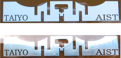
A UHF-RFID antenna pattern screen-printed using the developed aluminum paste (top),
and the antenna pattern provided with electrical conductivity by pressure annealing (bottom)
The pressure-annealed pattern has metallic luster. |
The importance of traceability of information on the origin and quality of a product is widely recognized due to increasing concerns for the safety of food and other products. Currently, a radio-frequency identification (RFID) tag, which wirelessly identifies and manages information on an object, plays an integral role in systems requiring traceability. Since RFID tags are often attached to goods, the production cost of the tag is included in the price of the goods. The production cost of the RFID tag must be reduced for widespread use of the tag in low-price goods.
The production cost of the RFID tag can be divided into two parts: a process cost and a material cost. Vacuum deposition and etching are used in the current production process of an RFID tag antenna and are the main contributors to the process cost. To reduce the overall production cost, it is being sought to change the production process from the currently used aluminum and copper vacuum deposition and etching processes to a resource- and energy-saving printing process. However, as conventional conductive pastes used in the printing process are made primarily of expensive silver, there has been a problem of increase in the material cost.
AIST has been conducting R&D of a pressure annealing technique to form inexpensive aluminum and copper conductive patterns on a flexible film (PET, polyimide, paper, etc.) by printing. The researchers have significantly reduced RFID tag production and material costs by applying the pressure annealing technique to the aluminum and copper pastes developed by Taiyo Holdings, and have successfully formed high-quality aluminum and copper UHF-RFID antenna patterns on a flexible film. An RFID tag in the UHF band can communicate with a transmitter/receiver located several meters away and can send and receive a large volume of information on goods at high speed.
Part of this research and development project was funded by Grant for Industrial Technology Research “Development of Technology for Non-thermal Sintering of Directly-imaged Metal Ink Patterns for Flexible Mounting” of the New Energy and Industrial Technology Development Organization.
Figure 1 shows the steps to form a UHF-RFID antenna pattern. First, UHF-RFID antenna pattern is screen-printed using the developed metal paste and the metal paste pattern is dried in a drying furnace. Then, the surface of the metal paste pattern is annealed to be electroconductive, while pressure is applied with a pressurizing head (pressure annealing). The pressurizing head is controlled so that pressure is applied vertically and horizontally to the metal paste pattern. In the pressure annealing process, the metal particles in the metal paste undergo plastic deformation and the metal oxide film at the surface of the particles breaks down, forming metal junctions between the particles. Since the surface of aluminum and copper particles is generally oxidized, it is difficult to form metal junctions between the particles. The pressure annealing technique can solve this problem.
 |
|
Figure 1 : Printing process for fabricating a UHF-RFID antenna pattern |
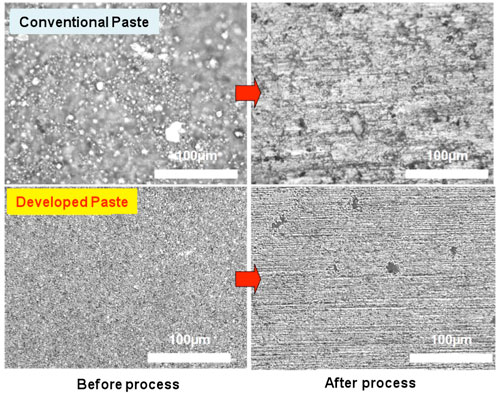
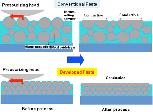
As shown in Fig. 2, when both the conventional and developed aluminum pastes are pressure-annealed, the aluminum particles are plastically deformed and the particle shape is not observable, indicating that metal junctions have been formed. However, the most significant difference between the two pastes is that the developed paste makes it possible to increase the filling rate of aluminum or copper particles in a printed film through design and control of the size distribution of the particles and use of a special dispersant. As a result, pressure can be uniformly applied to the surface of the printed pattern, resulting in a higher proportion of continuous conductive layer. When the conventional paste is used, pressure is not applied uniformly, resulting in a higher proportion of discontinuous conductive layer (Fig. 3). The electrical resistivity of the developed metal pastes significantly improved after pressure annealing with the resulting resistivity being roughly 1/5 (copper) and 1/7 (aluminum) compared to that of the conventional pastes (Table 1).
A thermosetting resin was used as the organic component of the pastes to improve the adhesion between the metal particles and the substrate. As a result, the adhesion to the substrate was stronger with the developed paste than with the conventional paste. In a standard tape peel test, strong adhesion was confirmed with no peeling. Generally, for low-temperature annealing conductive pastes, the annealing and hardening temperature must be set below 150 °C, the service temperature limit of PET. The use of pressure annealing makes it possible to lower the temperature of the production process. By setting the hardening temperature of the thermosetting resin below 150 °C, an antenna can be formed on a thermoplastic film such as a PET film, which has been difficult with conventional pastes.
(Reference: http://www.aist.go.jp/aist_j/press_release/pr2011/pr20111004/pr20111004.html)
 |
|
Figure 2 : Surface microscopic images of the conventional and developed aluminum pastes before and after pressure annealing |
 |
|
Figure 3 : Difference in conductive state after pressure annealing between the conventional and developed pastes |
|
Table 1 : Electrical resistivity achieved with the conventional and developed pastes |
 |
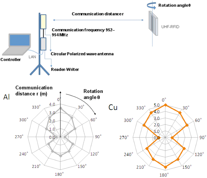
The transmission/reception characteristics of the pressure-annealed aluminum and copper antennas were evaluated by the measurement method shown in Fig. 4. The communication distance from the measuring device at a rotation angle of 0° is approximately 3.5 m for the aluminum antenna and approximately 5 m for the copper antenna, which are equal to or better than the existing UHF-RFID tag using a silver paste. The measured communication distance is the distance at which the recognition rate is 100%.
The thickness of the layer through which a surface current of 1 GHz passes, given the skin effect, is calculated to be 2.65 µm for aluminum and 2.06 µm for copper. Since the layer here is 2 to 3 µm thick, the communication distance decreases and the transmission/reception characteristics deteriorate, if the particles remain intact. Pressure annealing plastically deforms the particles at the surface of the metal paste and creates a very flat surface, enabling highly efficient transmission and reception. A strong correlation between the surface roughness and communication distance has been confirmed.
 |
Figure 4 : System for the measurement of the transmission and reception characteristics of the UHF-RFID (top),
and the characteristics of the aluminum and copper antennas (bottom) |
The researchers aim at the development of a pressure annealing system for a production line and at the practical use of aluminum and copper printed UHF-RFID tags. They will also investigate the application of the pressure annealing technique to the printing production of diodes, light-emitting devices, and solar cells.