Update(MM/DD/YYYY):02/03/2012
Development of a Copper Paste for Crystalline Silicon Solar Cells
- Replaces silver paste and accelerates the reduction in the cost of high-efficiency solar cells -
Points
-
The inexpensive copper paste achieves a performance nearly equivalent to that of conventional silver paste.
-
Adoption of the screen-printing low-temperature-sintering method results in low-damage high-efficiency manufacturing of solar cells.
-
Wiring and electrodes for various cell structures can be formed by printing through the adjustments in the alloy paste composition.
Summary
Hideo Tokuhisa (Senior Researcher), Manabu Yoshida (Senior Researcher) and others of Printed Electronics Device Team, the Flexible Electronics Research Center (Director: Toshihide Kamata) of the National Institute of Advanced Industrial Science and Technology (AIST; President: Tamotsu Nomakuchi), have succeeded in forming wiring and electrodes for crystalline silicon solar cells by applying a low-damage print manufacturing technology that uses the copper paste for low temperature process developed by Shigenobu Sekine of Napra Co., Ltd. (Napra; Representative Director: Junko Sekine).
Napra fabricated the copper paste by mixing copper powder and low-melting-point alloy particles that were produced using a method developed by Napra for manufacturing nano-composite particles. The particles are non-segregating and uniform. Use of the paste enables low-temperature sintering. AIST has realized the technology for high-productivity low-damage print manufacturing using the screen-printing low-temperature-sintering method.
These technologies enable low-cost print manufacturing of electrodes and wiring for crystalline silicon solar cells, while simultaneously satisfying the needs for low-temperature, low-heat-damage processing (<200 °C), low resistance (3×10⁻⁵ Ω·cm), low contact resistance (5.3×10⁻⁴ Ω·cm2), high peel strength, and high stability (oxidation resistance stability). They are also clearing a path for further low-cost production of solar cells. In addition, by controlling the composition of the alloy paste, these technologies can be applied to the formation of wiring and electrodes for various cell structures, including flexible displays and sensors.
Details of the technology will be presented at AIST Open Lab held in Tsukuba, Ibaraki, on October 13 and 14, 2011.
 |
|
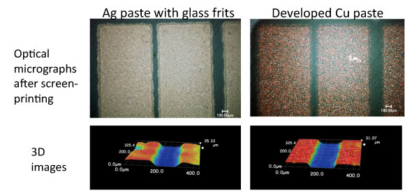
Structures of the silver paste currently used for crystalline silicon solar cells (left) and the newly developed copper paste (right) |
Social Background of Research
Social demand for the development and dissemination of solar cells as safe sources of energy has become quite high. Reducing cost is the most important challenge in popularizing solar cells widely in society. Cost reductions are achieved not only by improving cell efficiency, but also by lowering the cost of mounting process. Print manufacturing of electrodes and wires for solar cells by using silver paste has attracted high levels of interest in recent years. However, the price of silver used for the paste has risen sharply because of recent increases in global demand and the rapid popularization of solar cells, and there is an urgent need for the development of an inexpensive metal paste to replace silver.
Copper has attracted attention because of its electrical conductivity, which is almost equivalent to that of silver, and its price, which is two orders of magnitude lower than that of silver; however, in order to replace silver with copper, there are issues, such as the oxidation of copper and its diffusion into substrates. In addition, high-efficiency solar cells such as heterojunction solar cells require low-temperature manufacturing processes (less than 200 °C) to prevent thermal degradation.
There is a need for the development of a low-temperature-sintering-type printable copper paste to further reduce the cost of solar cells while improving efficiency.
History of Research
AIST has been developing device-manufacturing technologies using print processes with the aim of developing energy-saving, high-productivity manufacturing technologies for energy, information, and communication devices. It has developed flexible displays, flexible sensors, and flexible RFID (radio-frequency identification) tags by printing elements on flexible substrates such as plastic films.
Napra has used its original method to develop and mass-produce a low-melting-point alloy, which forms equiaxial crystals even after melting. The method involves the manufacture of nano-composite particles that are non-segregating and uniform. Napra has also used this low-melting-point alloy to develop a low-temperature-sintering-type alloy paste. AIST and Napra have examined the possible cost reduction by applying these technologies to the manufacture of crystalline silicon solar cells.
The present research and development have been conducted as part of “High Performance PV Generation System for the Future. R and D on Ultimate Wafer-based Si Solar Cells.” (FY 2010 to FY 2012), a project commissioned by the New Energy and Industrial Technology Development Organization.
Details of Research
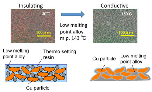
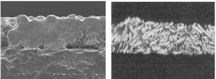
The copper paste developed by Napra is fabricated by mixing low-melting-point alloy particles and copper powder. The alloy particles were produced by the method for manufacturing nano-composite particles that are non-segregating and uniform. The low-melting-point alloy in the copper paste melts at a temperature lower than 150 °C (Fig. 1) and diffuses between and into the copper particles, improving the electrical conductivity by forming metallic bonds through alloying. In addition, low-melting-point alloy covering the copper particles suppresses the oxidation of copper particles and the diffusion of copper atoms into the substrate. Cross-sectional electron microscope images of the particles (Fig. 2) show that diffusion of the low-melting-point alloy into the copper particles forms a metal conductor with few gaps. In a conventional resin silver paste, the resin acts as a binder contacting the silver particles and thus helping to improve electrical conductivity. When the copper paste is used, the low-melting-point alloy acts as a binder, making the copper particles contact each other and improving the electrical conductivity.
 |
|
Figure 1 : Properties of the low-melting-point alloy before and after melting (structure and conductivity) |
 |
|
Figure 2 : Electron microscope images of the Napra-developed copper paste (left) and of commercially available resin silver paste (right) |
By using this copper paste, a conductor pattern was print-formed by a screen-printing process and was sintered at a temperature below 200 °C. It showed wire resistivity of 3×10⁻⁵ Ω·cm (Fig. 3); this was significantly lower than that of commercially available copper paste and comparable to that of commercially available silver paste. In addition, the researchers evaluated the contact resistivity by print-forming a pattern on an indium tin oxide transparent electrode, which is used in solar cells. It was found that the contact resistivity was lower (5.3×10⁻⁴ Ω·cm2) than that of silver paste used in the current solar cells. This will help to improve the efficiency of solar cells. The contact resistivity did not change after the print-formed pattern had been left in the atmosphere for more than half a year (7 months); high durability was confirmed. The fabricated electrode was evaluated by using a standard peel test (tape test) and exhibited highly adhesive properties with no trace of detachment. These results show that the developed copper paste is highly adaptable to the various demands of solar-cell manufacturing. The copper paste exhibits sufficiently high potential for replacing mainstream silver paste in the manufacture of solar cell electrode materials.
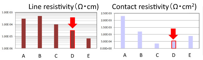 |
Figure 3 : Resistivity of silver and copper pastes
(Commercially available copper pastes: A, B, and C; Napra-developed copper paste: D; and commercially available silver paste: E) |
As described, the researchers have developed a print manufacturing technology by using low-temperature-sintering-type copper paste as the electrode component for crystalline silicon solar cells to realize the low-cost print manufacturing of such cells. This inexpensive paste has the potential to replace the currently used silver paste and thus promises to further reduce the cost of solar cells.
The current sintering temperature is set at 200 °C as the maximum heating temperature; however, optimizing the ingredients and the composition of alloy paste could enable lower-temperature sintering at temperatures as low as 143 °C, the melting point of the low-melting-point alloy. In addition, control of the ingradients will enable the adjustment in electrode work function and the manufacture of information terminal devices such as flexible displays and sensors with plastic film substrates, including PET (polyethylene terephthalate).
Future Plans
Aiming at prompt commercialization, the researchers plan to conduct environmental testing and to evaluate long-term durability and stability. They also aim at the early realization of cost reduction and efficiency improvement of high-efficiency solar cells by using the paste as an electrode material.