The researchers have developed a technology with which one can easily manufacture flexible circuit boards, that is, circuit formation by screen printing of copper ink, followed by newly developed cool plasma sintering.
 |
|
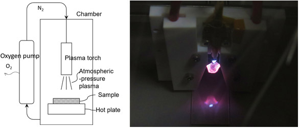
Fig. 1 Schematic of cool plasma sintering (left) and a picture showing the sintering with improved electrodes (right). |
 |
|
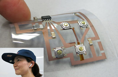
Fig. 2 Radio made by printing a circuit on a PEN film and mounting parts on it and an example usage where the radio has been put into the visor of a baseball cap. |
It had already been confirmed that copper nanoparticle inks for inkjet printing could be reduced and sintered on a polyimide film using cool plasma sintering (CPS). This time the researchers improved electrodes and the power supply for plasma generation to lower the processing temperature and developed a technology to screen-print uniformly by optimizing particle sizes of copper in the paste. This made it possible to manufacture circuit boards using a polyethylene naphthalate (PEN) film, which is less heat resistant, but inexpensive and transparent.
A lot of technologies are being developed in the field of printed electronics, which uses printing technology to manufacture electronic devices at lower cost with smaller quantities of resources. Copper has advantages over silver as a wiring material, as it is less expensive and causes fewer shorts due to migration. However, a sintering process for printed copper to reach low electrical resistance has not yet been established.
By improving the process speed of the CPS method, the productivity of flexible circuit boards using only copper ink printing and sintering will be raised to the same level as the conventional process (lithography technology) for possible mass production in three years.