Shingo Tamaru (Invited Senior Researcher), the Metal Spintronics Team, the Spintronics Research Center (SRC; Director: Shinji Yuasa), the National Institute of Advanced Industrial Science and Technology (AIST; President: Ryoji Chubachi) and Hitoshi Kubota (Principle Research Manager) and Akio Fukushima (Deputy Director), SRC, AIST, have developed a phase locked loop (PLL) circuit designed to stabilize the oscillation frequency of a spin torque oscillator (STO), and demonstrated generation of a highly coherent microwave signal from the STO.
The STO is a nanometer-scale magnetoresistive device that generates a microwave signal by applying a DC voltage. The 7.344 GHz microwave signal generated by the STO was phase locked to a 153 MHz reference signal by the developed PLL circuit, resulting in an extremely narrow spectral linewidth of below the measurement limit (1 Hz). The narrowest spectral linewidth of the microwave signal generated by a single magnetic tunnel junction (MTJ) based STO reported thus far has been 3 MHz achieved by AIST. The developed PLL circuit led to a dramatic improvement of the frequency stability of the STO oscillation. This accomplishment is expected to accelerate the progress toward the practical use of STOs as a voltage controlled oscillator (VCO).
Details of the results will be published in a scientific journal, Scientific Reports, published by Nature Publishing Group.
 |
|
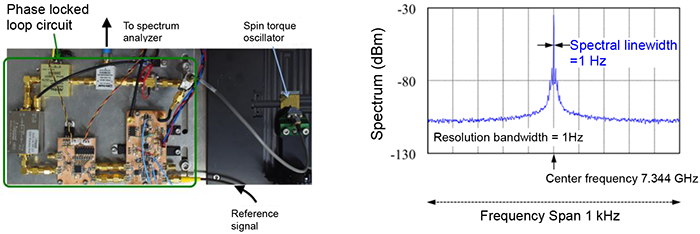
Photo of the developed PLL circuit and the spectrum of the microwave signal |
Recently, various microwave communication devices, such as cellular phone and wireless LAN, have been widespread, in which VCOs composed of semiconductor transistors and resonators are used. The resonator used in the conventional VCO has a size of as large as a few 100 μm, which is one of major obstacles for further miniaturization and cost reduction. On the other hand, the STO is a nanometer-scale magnetoresistive device requiring no external resonator, thus attracting significant attention as an ultra-small VCO compared with the conventional ones. However, the frequency stability of the STO is quite poor, hampering adoption of the STOs in real electronics systems.
AIST have been working on developing thin film deposition and microfabrication technologies for STOs by applying knowledge and experience gained through the research on spintronic memory devices. In order to use an STO in various practical applications, it has to show both large output power and high frequency stability. For this goal, the researchers have been focusing on realizing a stable oscillation of an STO based on MTJ, which has a high magnetoresistance ratio. They have already achieved the world highest output power at that time and the world best frequency stability of an output signal from a single STO (AIST press releases on Aug. 28, 2008 and Jan. 8 2014).
This work has been partially supported by the Grant-in-Aid for Scientific Research (S) “Research and Development of High Frequency Spintronics” of the Japan Society for the Promotion of Science.
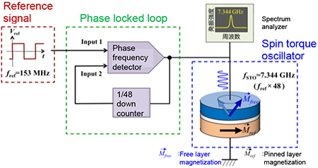
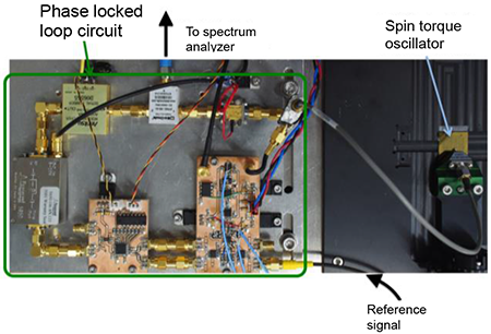
In order to realize a good enough frequency stability of an MTJ based STO for practical uses, the researchers improved oscillation characteristics of an STO and developed a PLL circuit designed to stabilize the oscillation frequency of the STO. The STO used in this work was fabricated out of a MTJ consisting of an ultra-thin MgO tunnel barrier of about 1 nm and amorphous magnetic alloy layers containing Fe. The interface between the MgO and magnetic alloy layer tends to align spins along the direction perpendicular to the interface plane. The spin precession trajectory was stabilized by utilizing this interface property. The oscillation frequency of this STO shifts lower as the applied voltage is increased. Figure 1 shows a block diagram and a photo of the PLL circuit. In this PLL circuit, the STO output signal is downcounted by 48, and its phase is compared with that of the 153 MHz reference signal. The phase difference between these two signals is converted to a voltage signal, and fed back to the STO to tune the oscillation frequency dynamically such that the phase difference is always minimized. The high frequency spurious signals contained in the feedback signal, which disturbs the STO oscillation, are blocked by a filter for stable feedback operation.
(a) |
(b) |
|
Figure 1: Developed PLL circuit using an STO as a VCO, (a) block diagram, (b) photo |
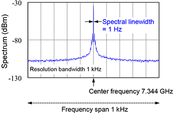
Figure 2 shows the spectrum of the output signal generated by the developed microwave oscillator. The center frequency is 7.344 GHz. The spectral linewidth, which represents the frequency fluctuation, is extremely narrow, below the measurement limit of 1 Hz, which clearly indicates the good frequency stability.
 |
|
Figure 2: Spectrum of the microwave signal generated by the developed microwave oscillator |
The oscillation performance of the STO, especially frequency tunability by voltage, will further be improved and PLL circuit design will be refined for higher frequency response in order to develop a higher performance STO based microwave oscillator. These efforts should lead to practical use of the STO as an ultra-small and low cost microwave oscillator.