- Atomic level structures near diamond surfaces play main roles in field-emission of electrons -
Yoshiyuki Miyamoto (Leader) of Nano-Carbon Materials Simulation Group and Takehide Miyazaki (Leader) of Nonequilibrium Materials Simulation Group, the Nanosystem Research Institute (Director: Tomohiko Yamaguchi) of the National Institute of Advanced Industrial Science and Technology (AIST; President: Ryoji Chubachi), and Daisuke Takeuchi (Chief Senior Researcher) of Energy Enabling Technology Group and Satoshi Yamasaki (Principal Research Manager), the Energy Technology Research Institute (Director: Katsuhiko Kadoguchi) of AIST, have examined efficiencies of field-emission of electron from diamond surfaces with different chemical modifications by performing first-principles calculations of electron dynamics. They found that the potential profile of electrons near the surface, which does not monotonically change as a function of the depth but shows complex modulation depending on the surface modification, plays a major role to determine the efficiency of the field-emission as well as the negative electron affinity (NEA) that was believed to be a key factor in enhancing the emission-efficiency for a long time. This theoretical finding is expected to accelerate experimental research aiming at improvement in field-emission characteristics and chemical stability when a diamond surface is chemically modified and at application research in the electron emission devices.
The details of this research will be published online in Applied Physics Letters on September 16, 2013 (EDT).
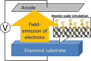 |
Schematic of the electric circuit that emit electrons from a diamond surface by applying bias voltage between a diamond substrate and an electrode (anode)
Atomic scale simulations which reflected the chemical modification of surface were performed. |
Diamond has high field-emission efficiency with relatively low operation bias voltage and thus expected to be applied as electron-beam sources which are used for measuring and improving qualities of nano-materials. Development of diamond electronic devices with a new mechanism that cannot be realized using silicon or other semiconductors has also been conducted. Chemical modification of diamond surfaces was considered to improve durability of field-emission devices but caused reduction in emission efficiency. Therefore fundamental understanding of the mechanisms that determine the field-emission efficiency was highly demanded. Chemical surface modifications which achieve NEA were believed to be a key for the high field-emission efficiency for a long time.
AIST has been conducting research and development of field-emission devices that can operate stably with low bias voltage through collaboration between experimental and theoretical research teams of electronic-device materials aiming at the development of high performance devices that cannot be realized by using conventional materials. The field-emission devices using diamond have superior performance, but the mechanisms of the field-emission have to be understood in order to achieve both high emission efficiency and chemical stability by mean of the surface modification.
This research was carried out in a project, "Ultra-high Voltage, High Efficiency, and Compact Vacuum Power Switch," as a part of "Advanced Low Carbon Technology Research and Development Project" conducted by Japan Science and Technology Agency. All calculations were performed by using computer resource of AIST, the AIST-Super Cloud – Generation2 (ASC-G2).
Hydrogen (H) termination of a diamond surface is a well known method to enhance electron emission from the surface into a vacuum that energetically stabilizes the system. By using this phenomenon, a vacuum power switch which works with a new mechanism (AIST press release on December 10, 2012) and a field-emitter were developed.
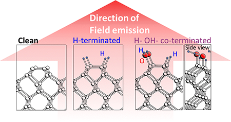
A theoretical understanding of emission efficiency of individual electrons considering an atomic level surface structure has been awaited to achieve further emission efficiency and chemical stability of the surfaces, because the conventional understanding was rather macroscopic considering electron affinities. Structures of several chemically modified diamond surfaces were determined by performing the first-principles calculations based on the density functional theory (Fig. 1), and the electronic affinities of these surfaces were examined at the atomic level. The calculations showed NEA for a H-terminated surface and a H- and hydroxyl (OH-) co-terminated surface, and positive electron affinity (PEA) for a clean surface. These results agree with past researches. Then field-emission simulations were performed for these surfaces by using the time-dependent density functional theory.
 |
|
Figure 1 : Structures of several chemically modified diamond surfaces considered in simulations |
The field-emission efficiencies of the diamond surfaces were compared by applying bias voltage on the surface and counting the number of electrons that emit into a vacuum as a function of time (Fig. 2). The emission efficiency of the H-terminated surface with NEA, is superior to that of the clean surface with PEA. This result agrees with past research results. However, the emission efficiency from the H- and OH- co-terminated surface with NEA was inferior to that of the clean surface with PEA. This strongly suggests that electron affinity cannot be a unique factor in determining the emission efficiency.
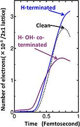 |
Figure 2 : Time-evolution of number of emitted electrons from diamond surfaces
The slope of each line indicates electric current from the diamond substrate to the anode. |
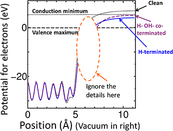
By investigating detailed profiles of potential for electrons at the surface region, the H- and OH- co-terminated surface has a region which tends to trap electrons, i.e. a potential well, on the way from the inside to the vacuum. The potential well originates from presence of surface oxygen atoms (Fig. 3).
Although the potential height of the H- and OH- co-terminated surface at the vacuum is lower than that of the clean surface, studying the electron dynamics revealed that the potential well prevents efficient emission of electrons.
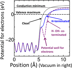 |
Figure 3 : Potential profiles for electrons on each surface
The profiles in directions parallel to the surface were averaged. |
In conventional consideration, the detail of the potential profile at the surface region was not taken into account, and only electron affinity was considered as shown in Fig. 4, i.e. only the potential difference between the inside region and the vacuum region determines the field emission efficiency. Accordingly, this conventional consideration results in the higher efficiency of the H- and OH- co-terminated surface than that of the clean surface. However, this conventional consideration assumes monotonic increase of potential for electrons from the inside to the vacuum region through the surface, and does not include detailed information of the atomic configuration due to chemical modification.
On the other hand, the current research used realistic models including structural information at the atomic scale. Then numerical simulations of electron dynamics taking detailed profile of potential for electrons into account were performed, which proved the H- and OH- co-terminated surface shows lower efficiency of field emission than that of the clean surface. The lower efficiency is due to presence of oxygen atoms which cause the potential well at the surface region (Fig. 3).
 |
|
Figure 4 : Schematic of conventional model which considers only relative heights of the potentials in the vacuum region and ignores the profiles at the surface region which are shown in Fig. 3 |
When simulations with an extend-sized model that can include surface roughness and defect-distribution become available, numerical simulations of the electron dynamics under an applied bias voltage can predict field emission efficiency depending not only on chemical surface modification but also on surface morphologies. By using the simulation results, the number of experimental try-and-error cycles can be reduced significantly and the research and development will be accelerated.