Tetsuya Tada (Leader) and others, Nanoscale Characterization and Processing Research Group, the Nanoelectronics Research Institute (Director: Seigo Kanemaru) of the National Institute of Advanced Industrial Science and Technology (AIST; President: Tamotsu Nomakuchi), have developed a three-dimensional stress analysis simulator for ultra-small silicon (Si) devices, in collaboration with Advanced Simulation Technology of Mechanics R&D, Co. Ltd. (President and Representative Director: Tomoaki Ando). The developed simulation technology allows the analysis of the distribution of the mechanical stress (or mechanical strain) applied to ultra-small Si devices with a spatial resolution at the nanometer level by calculating the modulation of light intensity distribution caused by the device structure in the micro-Raman spectroscopy measurement using an optical microscope.
The technology is expected to contribute to improving the speed and reducing the power consumption of leading-edge LSI devices, particularly three-dimensional FinFET devices which will be adopted at the 22 nm technology node.
The details of this technology will be presented at the 73rd Autumn Meeting of the Japan Society of Applied Physics to be held at Ehime University in Matsuyama, Ehime, on September 13, 2012 and at the 2012 International Conference on Solid State Devices and Materials to be held at Kyoto International Conference Center in Kyoto, on September 27, 2012.
 |
|
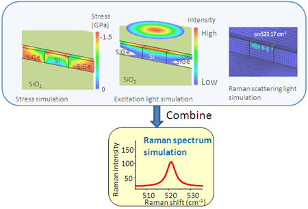
(Figure) : Schematic diagram of the developed simulation technology |
In the field of advanced semiconductor devices, higher speed and higher performance have been realized by intentionally applying stress to channel regions, in which carriers such as electrons and holes flow, to increase carrier mobility. If, however, there is any fluctuation in the stress, the performance of transistors fluctuates, making it difficult to sufficiently reduce operating voltage and, consequently, making it impossible to reduce power consumption. This is why it is necessary to suppress fluctuation in the stress in order to lower the power consumption of those devices. Against this background, a method to evaluate the stress distribution in a device with a high spatial resolution is needed in order to assess the influence of the stress on device performance, to clarify the relation between the device structure and the stress and, thus, to reflect such information in device structural designs and production processes.
In the MIRAI Project, AIST conducted the research and development of a measurement technology for local stress distribution in Si devices using micro-Raman spectroscopy. It has achieved world-class spatial resolution in a stress distribution analysis technology using Raman spectroscopy. For example, it has developed an evaluation technology for local stress distribution at a spatial resolution of 100 nm or less, which is shorter than the wavelength of light. During the research and development, it was found that the light intensity distribution in an ultra-small device was strongly modulated in the nanometer scale and thus the Raman spectrum was influenced heavily. In the present research, a method capable of evaluating quantitative stress distribution in the nanometer scale has been developed based on analysis by Raman spectroscopy reflecting the effect of light modulation, which is calculated with a simulation technology integrating electromagnetic field analysis and stress analysis, combined with technology CAD.
Part of the research and development was supported by "Millennium Research for Advanced Information Technology (MIRAI) Project" (FY2001 - 2010) commissioned by the New Energy and Industrial Technology Development Organization (NEDO).
Micro-Raman spectroscopy enables non-destructive stress measurement utilizing a phenomenon whereby, when excitation light incident on a sample is scattered, the wavelength of the scattered light shifts reflecting energy levels of lattice vibrations etc. Thus, micro-Raman spectroscopy is considered to be a promising method for evaluating stress distribution. Depending on the intensity and direction of the stress applied on a sample, the wavelength shift of Raman scattering light (Raman shift, which is normally expressed in wavenumber) varies. Accordingly, it is possible to qualitatively estimate stress by measuring the variation of Raman shift. However, because an optical microscope is used, the spatial resolution is limited to the wavelength of light (from several hundreds of nanometers to one micrometer). In addition, as stress is a physical quantity consisting of six independent components, quantitative evaluation of stress, including its direction and type, is difficult only with the Raman measurement. A conventional solution to this problem has been to evaluate stress distribution by comparing the results of stress simulations and micro-Raman measurements. In measurements of ultra-small devices, however, their device structure complexly modulates light propagation in the nanometer scale, causing a large influence over the measured Raman spectrum, and consequently, making it impossible to perform accurate stress analysis.
The developed simulation system combined the calculation of the propagation of excitation light and scattering light in a Raman measurement by electromagnetic simulation using the finite-difference time-domain method (FDTD) and stress analysis by the finite element method (FEM). This allows an accurate calculation of the Raman spectrum reflecting the nanometer scale modulation effect in light intensity distribution due to the device structure, and a quantitative calculation of stress distribution in the device.
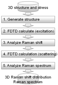
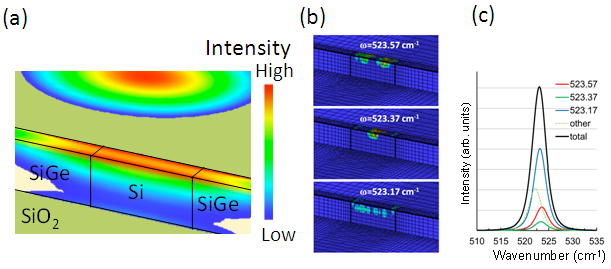
Figure 1 shows a flowchart of the developed three-dimensional stress analysis simulator. The overall structure consists of 1) the structure and stress reading unit (calculates stress distribution based on the FEM method); 2) the three-dimensional FDTD analysis unit (calculates the intensity distribution of excitation light); 3) the Raman shift analysis unit (calculates the wavelength of Raman scattering light from different points on a sample based on stress distribution); 4) the three-dimensional FDTD analysis unit (calculates Raman scattering light from the sample); and 5) the Raman spectrum analysis unit (calculates Raman spectra in wavelength regions actually measured). The analysis results are visualized by a three-dimensional viewer. Figure 2(a) shows the stress distribution of FinFET and the intensity distribution of excitation light calculated with the developed simulator. A Si channel formed on a silicon dioxide (SiO2) layer is under stress of a silicon-germanium alloy (SiGe) at both ends. The intensity distribution of excitation light is modulated by the sample structure; the intensity of excitation light close to the channel edge is especially strong, so the scattering light from the area close to the edge is significantly contributes the measured Raman scattering light. The excitation light is diffracted and illuminates the sidewall. Figure 2(b) shows the Raman scattering light of each wavelength from the Si channel. As the stress intensity varies depending on the location, the Raman scattering light is accordingly emitted at different wavelengths. Figure 2(c) shows the spectrum of each Raman scattering light obtained from the analysis and those spectra were combined to form a Raman spectrum. This combined spectrum is corresponding to the actually measured Raman spectrum. The stress analysis is adjusted until the difference from the measured spectrum disappears, and thus, the final value of stress is determined with the simulation.
 |
|
(Figure 1) : Flowchart of the developed three-dimensional stress analysis simulator |
 |
|
(Figure 2) :(a) Stress distribution of the FinFET structure and intensity distribution of excitation light calculated by the developed system; (b) Raman scattering light of each wavelength from the sidewall; and (c) Spectrum of each scattering light obtained from the analysis and the combined Raman spectrum. |
The spatial resolution of micro-Raman spectroscopy is generally limited to the wavelength of excitation light (from several hundreds of nanometers to one micrometer). On the other hand, the developed system, which makes accurate Raman simulations, is capable of estimating and evaluating stress distribution with a spatial resolution in the nanometer scale.
The researchers aim to make further contributions to society, such as commercialization of the Raman measurement system incorporating the developed measurement and evaluation technology.