- High-purity separation of SWCNTs with different carbon atom arrangements by simply pouring a dispersion solution onto a commercially available gel -
Hiromichi Kataura (Leader), Takeshi Tanaka (Senior Researcher), and Huaping Liu (Post-Doctoral Researcher), the Carbon Nanomaterials Research Group, the Nanosystem Research Institute (Director: Kiyoshi Yase) of the National Institute of Advanced Industrial Science and Technology (AIST; President: Tamotsu Nomakuchi), have developed a method for separating and collecting semiconducting single-wall carbon nanotube (SWCNT) species with different carbon atom arrangements by simply pouring the dispersion of SWCNTs into multi-stage gel columns.
The synthesis of SWCNTs yields a mixture of many chiralities, including metallic and semiconducting SWCNTs with completely different electric properties, and these semiconducting SWCNTs further consist of electrically different species. For electronic device applications, the mixture of electrically different SWCNTs needs to be separated into individual chiralities. While AIST has been working on SWCNT separation using gel, we have made an advance and developed an innovative method for SWCNT separation. This new method achieves the high-purity separation of electrically different semiconducting SWCNTs by simply pouring the SWCNT dispersion into multi-stage columns filled with gel. The dispersion agent is inexpensive, the gel columns can be used repeatedly, and the process can easily be automated. Thus, low-cost and large-scale separation would be possible.
This result will be published online in Nature Communications, a British scientific journal, on May 11, 2011 (JST).
 |
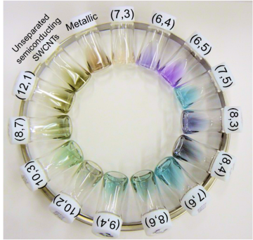
Figure : A total of 13 species of semiconducting SWCNT dispersion solutions were obtained from commercially available SWCNTs by the developed method. Each species has different electrical properties. The numbers in the photo indicate the indices that specify the chirality of each SWCNT species. Metallic SWCNTs and a mixture of unseparated semiconducting SWCNTs were also obtained. |
Note: This development has been conducted as part of the “Development of Irreplaceable Devices by Creation of the Second Generation Carbon Nanotube” (Research Director: Hiromichi Kataura) (FY2007-FY2012) in the research area, “Establishment of Innovative Manufacturing Technology Based on Nanoscience” (Research Supervisor: Yasuhiro Horiike, Emeritus Fellow, the National Institute for Materials Science), of the Core Research for Evolutional Science and Technology (CREST) of the Japan Science and Technology Agency (JST).
SWCNTs can have either metallic or semiconducting properties, depending on their carbon atom arrangement (chirality). Moreover, the “band gap” of semiconducting SWCNTs, which determines their electrical properties as semiconductors, varies depending on their carbon atom arrangement. SWCNTs are generally synthesized as a mixture of SWCNTs having such various electrical properties. In addition to applications for flexible transistors, it is expected that semiconducting SWCNTs will realize, in the future, a high-performance SWCNT computer with ultra-high integration and ultra-high speed. However, since mixtures of many kinds of semiconducting SWCNTs having different electrical properties do not fully exhibit the intrinsic high performance of SWCNTs, it has become necessary to develop a high-purity chirality separation technique that is capable of separating only semiconducting SWCNT species having the same chirality and hence the same electrical properties.
At present, since there is no method to synthesize specific SWCNTs having particular electrical properties, there have been various efforts to separate SWCNTs with individual chirality from the mixtures. However, with the existing techniques, it is extremely difficult to perform high-purity chirality separation and refinement on a large scale, as they require careful treatment for a long time and expensive reagents. Thus, the development of a new separation technique that enables high-purity, low-cost, and large-scale processing has been desired.
Until now, AIST has developed various separation techniques, such as: the high-yield separation of metallic and semiconducting SWCNTs by applying gel electrophoresis on “SWCNT-containing gel” that contains SWCNTs embedded in an agarose gel (AIST press release on February 26, 2008); separation without using an electric field (AIST press release on March 4, 2009); and a large-scale separation method using an agarose gel column (AIST press release on November 27, 2009). This time, we have further advanced this research to develop an improved technique for SWCNT separation.
With the already developed technique for separating metallic and semiconducting SWCNTs using agarose gel, efficient separation has been achieved by utilizing the phenomenon discovered by AIST in which the agarose gel selectively adsorbs semiconducting SWCNTs. However, with this technique, it was difficult to further separate semiconducting SWCNTs depending on the difference in carbon atom arrangement.
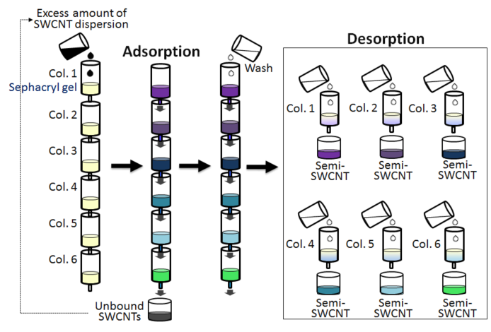
This time, we have developed a new separation technique that solved this problem by using commercially available Sephacryl gel. We have discovered a phenomenon in which the selective adsorption of SWCNTs with a specific carbon atom arrangement occurs by loading an excess amount of SWCNT dispersion onto Sephacryl gel. The varied adsorption strength between SWCNTs and the gel depending on their chiralities was inferred as the cause of this phenomenon. Based on this finding, we have invented a gel column-separating technique that uses a new concept, where multiple columns are arranged in series, each filled with a small amount of the gel, and in which an excess amount of SWCNT dispersion is poured into the columns (Fig. 1).
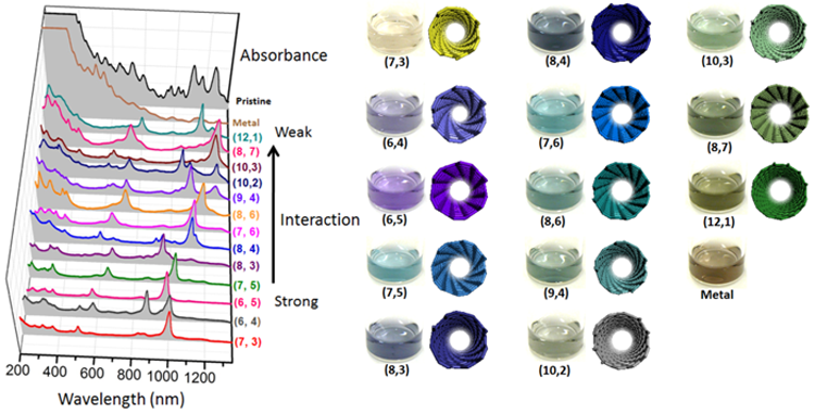
The first column of the multi-stage columns adsorbs only the semiconducting SWCNT species having a structure most easily adsorbable by the gel, and the remainder is poured onto the second column. The second column adsorbs the semiconducting SWCNT species having the most easily adsorbable structure among the SWCNTs not adsorbed by the first column (i.e., the second most adsorbable structure). In this manner, the first column adsorbs the most adsorbable semiconducting SWCNT, the second stage the second most adsorbable semiconducting SWCNT, and so on. Eventually, by eluting each column that has selectively adsorbed specific semiconducting SWCNT species, we collect different semiconducting SWCNTs each having different chirality. This time, we have successfully separated 13 species of predominantly single-chirality SWCNTs by re-separating the SWCNT dispersions obtained from the first round of chirality separation (Fig. 2).
 |
|
Figure 1 : Schematic diagram of the chirality separation of SWCNTs by overloading the multi-stage columns |
|
In this example, six-stage columns are used. Each of the six-stage columns is filled with a small amount of gel, a SWCNT dispersion solution is overloaded onto the column, excessive SWCNTs are washed away, and chirality-separated SWCNTs are collected by eluting each column. By repeating the six cycles of feeding the dispersion solution flowed through the last column back onto the top of the six-stage columns, this system practically works as 36-stage columns stacked in series. |
 |
|
Figure 2 : 13 species of single-chirality SWCNT dispersion solutions (right) and absorption spectra of the dispersions (left) |
|
The absorption peaks at the right side correspond to the band gap transitions, each of which has a different value. The spectra are arranged in the order of interaction strength between the species and the gel, with the strongest at the bottom. |
Most of the existing separation techniques extract only a part of SWCNT raw materials. In contrast, with the developed separation technique, the raw materials are divided into fractions, and thus almost all input SWCNTs are separated and collected without loss. In parallel with the high-purity chirality separation of semiconducting SWCNTs, separation into metallic and semiconducting SWCNTs is performed, and high-purity metallic SWCNTs are separated and collected. In addition, semiconducting SWCNTs not separated into single chiralities are collected as high-purity semiconducting SWCNTs, which are good enough for the applications that do not require the extremely high performance of single-chirality SWCNTs.
With this separation technique, only the commercially available gel that is capable of being used repeatedly and an inexpensive surfactant are needed, and the process where the dispersion solution simply passes through the gel can easily be automated. This will enable us to achieve low-cost and large-scale separation. In addition, the negligible loss of the raw material and the small amount of energy required for the separation process provide for an energy-saving separation technique.
We will strive to establish a mass production technology, and in 10 years, we will develop practical applications for single-chirality semiconducting SWCNTs as next-generation semiconductor materials. In the meantime, we are looking for partner companies to work together on the development of practical applications.