Update(MM/DD/YYYY):12/28/2007
First Cryptographic Hardware Validated by JCMVP®
- Improves the security of cryptographic products and contributes toward international standardization procedures -
Points
-
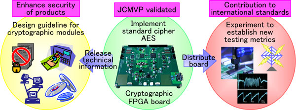
This is the first cryptographic hardware validated by the Japan Cryptographic Module Validation Program (JCMVP®).
-
The details of the cryptographic field programmable gate array (FPGA) board will be released to provide guidelines for designing cryptographic hardware with high security.
-
This FPGA board used as a standard hardware platform will provide uniform experimental environment for domestic and foreign universities and research institutes, and it will contribute significantly toward the international standardization of new security testing and metrics for cryptographic modules.
Summary
Akashi Satoh (Senior Research Scientist), the Research Team for Physical Analysis (Leader: Kentaro Imafuku), the Research Center for Information Security (Director: Hideki Imai) of the National Institute of Advanced Industrial Science and Technology (AIST) (President: Hiroyuki Yoshikawa), and Takafumi Aoki (Professor) and Naofumi Honma (Assistant Professor) of the Graduate School of Information Sciences, Tohoku University (President: Akihisa Inoue) have jointly developed an FPGA board integrated with a cryptographic function.
The newly developed FPGA board was validated by the Japan Cryptographic Module Validation Program (JCMVP®), which is managed by the Information-Technology Promotion Agency, Japan (IPA®), as the first cryptographic hardware module.(December 17, 2007) The cryptographic FPGA board with the international standard cipher algorithm Advanced Encryption Standard has obtained a certificate for level-1 security.
AIST will distribute the newly developed FPGA board as the standard board for testing to domestic and foreign universities and research institutes free of charge in order to establish a new security testing and metrics for cryptographic modules. AIST will also release the detailed design specifications and source codes of the board on a website as the design guidelines for cryptographic hardware. These measures will promote popularization of cryptographic products evaluated by third parties, and will contribute to improve security of entire information systems and products.
 |
|
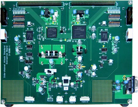
Gneneral picture of the cryptographic FPGA board
|
Social Background of Research
With the rapid expansion of broadband networks and the spread of information appliances, IC cards, and radio frequency identification (RFID) tags, etc., large amount of data are transferred in every phase of daily life; at the same time, security threats such as leakage and falsification of information are increasing. Cryptography is widely used even in consumer products as the fundamental technology to counter such threats. However, it is difficult for users to determine whether or not the cryptographic algorithm is properly implemented. It is not unusual that a security flaw is found in a product that is featured to possess perfect security measures.
Under these circumstances, the Japan Cryptographic Module Validation Program (JCMVP®) managed by IPA® was officially launched in April 2007. This is a third-party evaluation and validation program for cryptographic modules to ensure that the cryptographic algorithms are correctly implemented in products and the security sensitive information such as the cryptographic key and password is protected.
The distribution of products with assured security is essential to establish secure and safety information networks; however, high degree of expertise is required to develop cryptographic hardware that is acceptable by the third-party evaluation. It has been strongly desired to release detailed information and source codes of validated cryptographic modules as an implementation guideline. However, the detailed implementation information of cryptographic hardware that is the core of security products has not yet been released.
The National Institute of Standards and Technology (NIST) of U.S.A. is currently working to revise their testing metrics, and international standards are also being scheduled to be revised. Although constructing a uniform testing environment is vital for the formulation of international standards, it is difficult to standard evaluation schemes proposed by each research institute because they use their own experimental equipments, and thus third parties may not be able to verify the results.
History of Research
The Research Center for Information Security of AIST has been developing the high-performance cryptographic hardware implementation and conducting research on security evaluation scheme for cryptographic products, such as IC cards. It takes initiative in the Cryptography Research and Evaluation Committees (CRYPTREC), which is jointly managed by IPA® and the National Institute of Information and Communications Technology, and in the working group of power analysis experiments to establish security and testing requirements for cryptographic modules using e-Government recommended ciphers.
This validated FPGA board was developed as part of the research on the “Evaluation Scheme of Physical Attacks on Cryptographic Modules,” which is a project sponsored by the Ministry of Economy, Trade and Industry.
Details of Research
The newly developed cryptographic FPGA board (Figure 1) with the standard cipher algorithm AES encrypts and decrypts data transferred from a PC connected to this board.
Because the FPGA is a reconfigurable LSI, the circuit may be modified and confidential information may be stolen by means of attacks. Also, data might not be decrypted because of malfunction of the circuit. Hence, we developed tamper-resistant and error-detection functions to satisfy the security requirements specified in the international standard (ISO/IEC 19790) and implemented them on this FPGA board. AIST will release the specifications of the cryptographic FPGA board, circuit diagrams, and all of the source codes implemented on the web page (http://www.rcis.aist.go.jp/special/SASEBO) for free.
 |
|
Figure 1. The cryptographic board with the AES cipher, which was validated by JCMVP
|
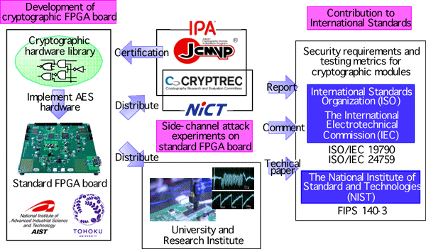
In addition, this FPGA board is used as the experimental board to establish new testing metrics and to evaluate their usefulness, and thus the board can precisely measure the power consumption and electromagnetic waveforms generated by the cryptographic circuit. This board will be distributed to domestic and foreign universities and research institutes as a standard evaluation board, and will contribute to promote research activities on new testing scheme and to revise the international standard for cryptographic modules. (Figure 2)
In order to correct a large amount of useful experimental data, standard hardware designs of cryptographic algorithms are required, which are implemented on the FPGA board. Because the design of cryptographic circuit is a very valuable intellectual property, source codes have rarely been released so far. AIST and Tohoku University designed all the ISO/IEC standard cryptographic circuits including the AES cryptographic circuit on the FPGA board, and will release the source codes on the above mentioned web page for free.
 |
|
Figure 2. Research and international standardization activities taking advantage of the standard evaluation FPGA board.
|
Future Schedule
AIST will develop a special LSI board that contains all the cryptographic algorithms of the international standard (ISO/IEC 18033-3) and an FPGA board with a different architecture. The FPGA of each board has microprocessor functions, and experiments on cryptographic software as well as cryptographic hardware will be performed.
AIST will distribute this FPGA board as the standard board for security evaluation and will release the design information of cryptographic hardware and software to improve the experimental environment and to standardize evaluation methodology. Through these activities, AIST will promote the cryptographic module validation program and will contribute to the revision process of the international standards.