The Power Electronics Research Center (PERC) of the National Institute of Advanced Industrial Science and Technology (AIST), , has succeeded in the on-resistance of 4.3 mΩcm2 and blocking voltage 1100 V in a transistor structure developed by the PERC-AIST, named “implantation and epitaxial MOSFET (IEMOS) with high channel mobility of normally-off type SiC power MOSFET.This resistance value is smallest in the world, as small as 1/5 that of the insulated gate bipolar transistor (Si-IGBT), a power device used widely at present. The power loss at the time of operation is also 1/5 as small. The newly developed device will be applicable to switching power supply, air conditioner, uninterruptible power source (UPS), inverter for electric or hybrid vehicle, and so on. In these applications, switching loss inherent to conventional Si-based devices will be extensively reduced, saving energy in home electric appliances to break through the technological limitations, and opening the way to new generation switching devices for energy saving and eco-friendliness.
In SiC power MOFET, called double-implanted MOSFET (DIMOS), SiC reigionnamed P well in contact with gate oxide film (Figs. 3 and 5) is formed by aluminum implantation followed by heat treatment at 1600 °C or higher, which induces Si to evaporate from the flat SiC surface to make it rough (Fig. 4). Electrons flowing through this region are disturbed by scattering at the roughness to increase on-resistance. On the other hand, in the IEMOS developed by PERC-AIST, the surface of P well prepared by epitaxial growth is flat without heat treatment at 1600 °C or higher (Fig. 6), letting electrons flow smoothly to reduce On-resistance to 4.3 mΩcm2, the smallest value in the world. The bottom of P well is formed by high concentration implantation, with N- type region designed to high blocking voltage, the device is successfully made the blocking voltage 1100 V or higher. Moreover, the device is of normally-off type admitting no current when no gate voltage is applied , allowing gate control readily when used with general inverter.
While on-resistance of Si-IGBT with blocking voltage of 1000V widely used at present is around 20 mΩcm2 , that of IEMOS is 4.3 mΩcm2, 1/5 as small as that of Si-IGBT, which is of bipolar type with certain demerits such as slow switching speed and large power loss at the time of switching. The newly developed SiC-IEMOS is of unipolar type, and is characterized not only by small on-resistance, but also by high switching speed.
Details of the present study will be reported at the 52nd Spring Meeting,2005, The Japan Society of Applied Physics and Related Societies to be held at the Saitama University from March 29 to April 1.
The present R&D work has been carried out as a part of the project “Strategic Development of Technology for Rational Energy Utilization” entrusted to AIST by the New Energy and Industrial Technology Development Organization (NEDO), under a grant from the Ministry of Economy, Trade and Industry (METI).
 |
|
|
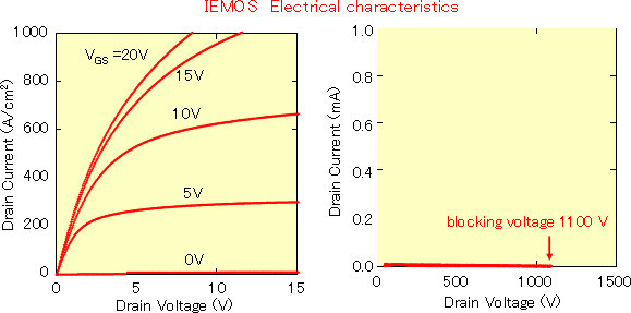
Fig. 1 Current-voltage characteristics of newly developed IEMOS
on-resistance (voltage/current) = 4.3 mΩcm2
Vd = 1 V, Vg = 15 V (3 MV/cm)
|
|
Fig. 2 Reverse characteristics of newly developed IEMOS
No current flows up to 1100 V, but a large current flows beyond that to break down the device.
|
With SiC device, it is theoretically possible to reduce on-resistance to two orders of magnitude in comparison to that of existing Si device. The use of SiC device is expected to reduce power loss extensively, when applied to - home appliances such as air conditioner and IH heater, semiconductor devices for on-vehicle use, and high power conversion device for distribution grid. SiC substrates are being marketed from suppliers of Japan, Europe and the United States. The SiC industry is being established with the supply of 3” substrate. Usually, in air conditioners and IH heaters, switching devices such as power MOSFET or IGBT are used in combination with rectifier devices such as Schottky barrier diode (SBD). Among them, on-resistance of SiC-SBD is as small as the theoretical minimum. SiC-SBD has been put to market by German and US company , aiming at a business deployment. On the other hand, SiC power MOSFET is expected to be used as switching device owing to small on-resistance and fast switching speed. While on-resistance of SiC device is smaller than that of Si device, it is much larger than the theoretical limit, preventing full performance of SiC device from being exhibited, when used in air conditioners or IH heaters. High on-resistance of the SiC power MOSFET is attributed to high channel resistance which takes the major part of on-resistance.. In contrast to the Si device, high resistance of SiC device may be accounted for by the existence of defects in high density at the interface (boundary) between the gate oxide film and P well, and roughness in channel area below the gate oxide film to disturb the current flow. It has been urgently requested to develop serviceable SiC power MOSFET in order to reduce the power consumption by applying low loss SiC power devices in various home appliances and industrial equipment.
In typical power SiC-MOSFET named DIMOS (Fig. 3), P-type SiC domain (or P well) in contact with the gate oxide film is formed by aluminum implantation followed by heat treatment at temperatures higher than 1600 °C. The heat treatment makes the flat surface of SiC rough with Si evaporated (Fig. 4). The current flow is impeded through scattering of electrons by collision at the roughness to raise the on-resistance. The PERC-AIST has developed an original SiC device of innovative construction, implantation and epitaxial MOSFET (IEMOS), with high concentration ion implantation at the bottom of P well and epitaxial layer at the top (Fig. 5). The epitaxial layer at the top is formed through chemical reaction between silane and propane without heat treatment to activate aluminum. This keeps the SiC surface flat (Fig. 6) to ensure smooth flow of electrons, achieving the world record on-resistance of 4.3 mΩcm2 (Fig. 7). Besides, the blocking voltage as high as 1100 V has been attained through the structural design between the high concentration layer provided by implantation at the bottom and the P well (Fig. 6). On-resistance of SiC power MOSFET is shown in Fig. 7, realizing a SiC power MOSFET of highest performance in the world. (Recently, ROHM CO., LTD announced DIMOS of 7.15 mΩcm2 and 1030 V.) The IEMOS is of normally -off type which admits no current when gate voltage is not applied, and widely used in the area of power electronics. The advent of such a general purpose device will exerts a great impact to power electronics. The on-resistance of IEMOS, 4.3 mΩcm2, is 1/5 as small as that of Si-IGBT, known to have the lowest on-resistance (about 20 mΩcm2) among Si devices. While the Si-IGBT is of bipolar type with large switching loss and slow switching speed, the newly developed SiC-IEMOS, of unipolar type, is characterized by small switching loss and fast switching speed.
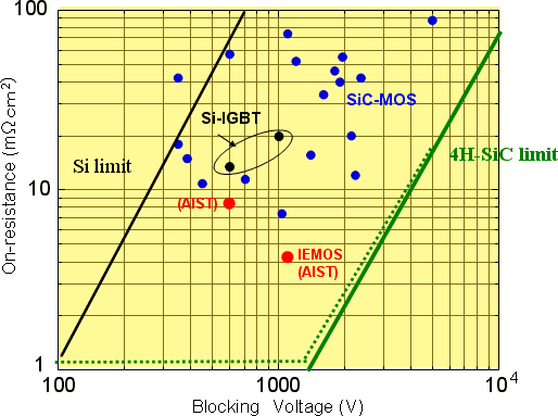 |
Fig. 7 Relationship of on-resistance to blockingvoltage |