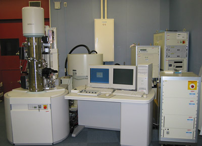
The Research Center for Advanced Carbon Materials of the National Institute of Advanced Industrial Science and Technology (AIST), one of independent administrative institutions, succeeded in developing an elemental analysis equipment of highest sensitivity in the world in collaboration with Hitachi High-Technologies Corporation (to be designated as Hitachi HiTec hereinafter). The equipment consists of a scanning transmission electron microscope (STEM) and an electron energy loss spectrometer (EELS), and its detection sensitivity is an order of magnitude better than that of the existing elemental analysis equipment, allowing to identify individual atoms.
It has been often noted that the property of nano-materials such as carbon nanotube is markedly affected by the presence of a single impurity atom. For the study of bio-polymer, such as direct readout of amino acids sequence of protein, the identification of at the level of single atom is essential. In this way, the technology to identify single atoms constituting nano-materials or bio-polymers has been sought for one of generic technologies covering nano-technology and bio-informatics.
Except for a few cases, the elemental analysis at atomic level has never been achieved in the world with a general-purpose equipment. The newly developed equipment produces focused electron beam of 0.2 to 0.3nm diameter (1nm=1/1,000,000,000m) from the STEM, which probes a subnanometer area to pin down atom species included there in combination with the EELS.
Factors contributing the achievement of this feat involve the use of newly designed high performance magnetic lens making it possible to focus electron beam into finer size and allowing greater probe current into the beam, and newly developed detector with improved coupling interface. The sensitivity of the new equipment is one order of magnitude better than that of the conventional one.
It is expected that the success of elemental identification at the atomic level will open the way to “the development of nano-devices and–materials requiring exact control of impurity or dopant quantity” or to “molecular labeling analysis replacing a particular part of bio-polymer with specific element”.
* The result of this study will be published on line at the website of a science journal, Proceedings of the National Academy of Sciences of the United States of America (PNAS) in the week of May 31, 2004.
* Works on the development of new materials based on the study, carried out at the University of Tokyo (UOT) and other organizations will be announced to the press from UOT.
 |
Fig. 1. Chemical analysis equipment of world’s highest sensitivity
An outer view of the chemical analysis equipment developed by the collaboration between NCRC-AIST and Hitachi HiTec. The equipment consists of a scanning transmission electron microscope and an electron beam energy loss spectrometer, realizing a detecting sensitivity one order of magnitude higher than that of the conventional equipment. The system is expected to contribute to the detection of trace impurities in semiconductor materials and to molecular labeling analysis for bio-polymer by replacing a particular site of it with specific element. |