– Efficient production of a variety of sensors and acceleration of IoT development –
The researchers have developed a printing technology named “Lift-On Offset Printing” that can fabricate a suspending microstructure, such as a cantilever and a bridge, within a short time frame and at low cost.
 |
|
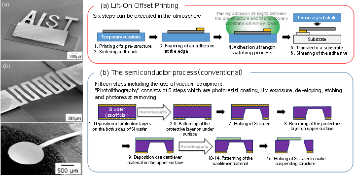
Photos of cantilevers and other micro structures, and schematics of the processes of cantilever fabrication |
The researchers have developed a process for fabrication of a suspending microstructure in which a microstructure is built on a temporary substrate by using an offset printing process. It is then separated from the temporary substrate by reducing its adhesive power, and the microstructure is bonded to a new substrate. This process allows a microstructure to be fabricated at atmospheric pressure and reduces the fabrication time to one-fifth of that in a semiconductor manufacturing process.
Sensors such as cantilevers that have suspending structures and use displacement of the structures, such as deflection, are utilized for position detection in smartphones and can be used in a wide variety of other applications, including detecting physical quantities, such as pressure and acceleration, and adsorption of chemical substances. The amount of deflection can be adjusted by changing the width, thickness, or material of the suspending structure, enabling a wide range of sensitivities. The semiconductor manufacturing process that has been used up to now has problems: it involves many steps and generates a large amount of waste; it also requires a substrate with high precision and durability, making it difficult to achieve efficient and low-cost production.
The performance and variety of sensors will be increased by allowing a variety of materials to be used. The print area will be increased and a mass-production process will be established. This technology will be transferred to private companies to help achieve a safe and secure society.