– Terahertz absorptance above 99%, more than double in high-speed responsivity compared with conventional absorbers –
Researchers) KUWANO Genki, Researcher, HOKARI Ryohei, Senior Researcher, KURIHARA Kazuma, Research Manager, Advanced Manufacturing Research Institute, TOJIMA Yuya, Researcher, KINOSHITA Moto, Group Leader, Research Institute for Physical Measurement
- Absorption structures converting terahertz waves into heat with fast thermal response
- Hollow pyramidal structure with three-dimensional thermal path fabricated by 3D printer and deposition technique, achieving both high absorptance and fast thermal response
- Component for highly efficient terahertz power sensors for next generation communication system

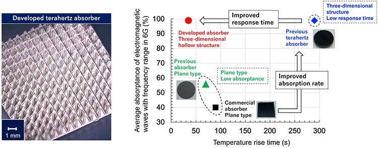
Microscopy image of developed terahertz absorber (left) and comparison of specifications with previous absorbers (right).
6G has received extensive attention in next-generation communication infrastructure to realize Society 5.0, where all people and things will be connected to create unprecedented value (see Beyond 5G/6G White Paper by the National Institute of Information and Communications Technology (NICT)). Terahertz power sensors are promising components to realize 6G in addition to semiconducting transmitter/receiver devices. To use the terahertz sources and detectors in 6G, characterization and calibration are important to provide reliability.
A reliable test with high accuracy is required because solid-state terahertz sources suffer from low emission power, and it is difficult to achieve threshold power needed for a communication system. It is also important to realize fast characterization to examine the power dependence with respect to current-voltage characteristics as well as emission frequency.
Highly efficient power sensors have been developed in the visible, infrared, and specific terahertz regions. However, in the frequency range in 6G, power sensors with the same or better specifications compared to the visible and infrared ones remain undeveloped. This is caused by the low absorptance of the absorber, which affects the accuracy of sensors. Even if the absorptance is improved by using a three-dimensional structure, such as a pyramid structure, the increase in volume delays the temperature rise time of the absorber and reduces the response time of the sensor. Hence, the development of an absorber with high absorptance and fast thermal response, and superior productivity enables us to design highly efficient power sensors. This leads to providing terahertz power sensors to users in general as well as to measurement manufacturers. This helps us to realize next-generation communication technology using terahertz waves.
AIST researchers have developed a terahertz absorber with high absorptance and fast thermal response, as well as superior productivity.
Terahertz power sensors determine the absolute power of incident electromagnetic (EM) waves through temperature rise in an absorber which coverts EM energy into heat. Therefore, an absorber with high absorptance and fast thermal responsivity enables us to realize accurate power measurement with fast response time. However, in the frequency range in the 6th generation mobile communication systems (6G), how to achieve both high absorptance and fast rise in temperature remains an open challenge. In this study, we proposed a three-dimensional hollow structure that achieves both high absorptance and fast temperature rise, and fabricated an absorber using a 3D printing and electroless plating technique. Its evaluation result showed that absorptance more than 99% was achieved in the frequency range in 6G, and the temperature rise time was more than twice in comparison with conventional absorbers. This technology will allow us to develop terahertz power sensors with high accuracy and fast response time. The highly efficient power sensors help us to spread next-generation communication technology using terahertz waves.