– Aggressive integration through Si/Ge stacked channel heterogeneous complementary field effect transistor (hCFET) –
Owing to the explosive spread of IT devices, there is a huge demand for high performance and low power consumption of integrated circuits. Ge possess higher hole mobility than that of Si and can operate under lower gate voltage. Therefore, the CMOS technology composing of a Si nFET and a Ge pFET is strongly needed.
In 2001, AIST started the research on high performance Ge transistors. On the other hand, the development of 3-dimensional ultra-scaled process technology for beyond the 2nm node has strongly been pushed by the Taiwan Semiconductor Research Institute (TSRI), Taiwan. In 2018, the international collaboration between AIST and TSRI started.
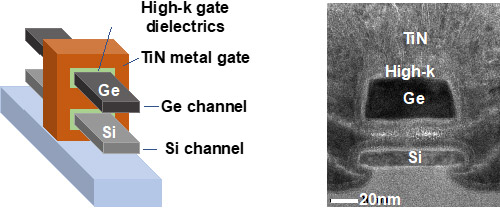
Through the international collaboration between Japan and Taiwan semiconductor research institutes, the researchers fabricated a Si nFET /Ge pFET vertically stacked heterogeneous complementary field effect transistor (hCFET) for the 2nm node. By utilizing hetero-layer boning technology, a Si nFET and a Ge pFET can be stacked and connected with the shortest distance in the hCFET. This ultimate new device architecture can lead to the realization of higher performance and lower power consumption CMOS devices. The detail of this technology will be presented in the 2020 International Electron Device Meeting (IEDM 2020).

Si/Ge channels stacked heterogeneous complementary field effect transistor (hCFET)