Dr. Takeru Amano et al. of the Ultrafast Optoelectronic Device Group in the Photonics Research Institute (Director: Masanobu Watanabe) of the National Institute of Advanced Industrial Science and Technology (AIST, President: Hiroyuki Yoshikawa) have produced the highest density and most uniform quantum dots in the world. Using these quantum dots they have manufactured a communication semiconductor laser which has a large modal gain due to the high density.
Semiconductor lasers using quantum dots with high quantum efficiency have been thought to have promise as a new light source. However, because of their low dot density conventional quantum dot lasers do not have sufficient modal gain, and special structures such as high-reflection film mirrors and long resonators are necessary. This has made practical use of the quantum dot lasers difficult.
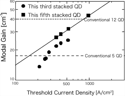
In this work, using As2 molecular beams developed at AIST, and gradient-composition strain relaxation layers, the world's first manufacturing of high density (1 x 1011 cm-2) and high uniformity (half width: 23 meV) quantum dots has been made possible. By applying the quantum dots to semiconductor lasers, we have succeeded in inducing laser oscillation at the 1.3 µm waveband without special laser structures. Furthermore, we have attained a modal gain characteristic of over 40 cm-1, the best in the world, using five stacked layers, which is less than half the conventional number of stacked layers (Fig.1). Hereafter, we will aim at high-speed operation. If, using the high density and high uniformity quantum dots we have developed, high-speed operation beyond 40 GHz, which is currently the fastest in the world, is theoretically possible.
Our invention is a breakthrough in techniques for developing quantum dot lasers capable of high-speed operation. We expect that if such high-speed quantum dot lasers can be made practicable, we will be able to enjoy high quality images, which need high speed communication to be delivered, at home.
 |
|
Figure 1 Large light amplification
|
Recently, the promise of large-capacity optical communication networks at short and intermediate distances has been increasing because of the explosive increase in communication capacity. For light sources for optical communication at short and intermediate distances, much attention has been paid to materials emitting light at the 1.3 µm waveband, the zero-dispersion waveband of optical fibers. InAs quantum dot structures produced with inexpensive GaAs substrates can emit 1.3 µm light, and thus the development of semiconductor lasers with the dot structures has been hoped for.
Furthermore, as quantum dot lasers have excellent characteristics, such as high quantum efficiency, temperature independence, etc., a reduction in cost and electricity consumption can be expected. This suggests that the quantum dot lasers are applicable not only for light sources for short and middle distance optical communication, but also to various fields utilizing optical interconnects, such as communications between computers or boards.
However, as the surface density of conventional quantum dots is low, approximately 1 x 1010 cm-2, and accordingly the number of manipulable carriers is low, sufficient optical magnification cannot be attained.
For this reason, such structures as high-reflection film mirrors and long resonators are needed to induce the oscillation of the lasers, resulting in a significant problem for the performance of communication lasers (e.g., the modulation speed). The increase in the number of the quantum dots contributing to light emission is very important to obtain large modal gain, and thus the production of high density and high uniformity quantum dots has been expected.
In AIST, research and development of optical and electronic devices utilizing quantum effects has been carried out to create new optical and electronic devices. In particular, investigation on the structures of quantum wires and quantum dots using As2 molecular beams has actively been executed. In this work, gradient-composition strain relaxation layer structures were used, together with the As2 molecular beams we developed.
Using these techniques, we have developed the highest density and most uniform quantum dots in the world. We have also fabricated a semiconductor laser with the quantum dots, and succeeded in laser oscillation without using a high-reflection film mirror and long cavity structure. In addition, we have attained a modal gain performance which is in the top class of the world standards. This study was carried out with the support of the Strategic Creative Research Promotion Project by the Science and Technology Promotion Bureau.
We produced high density and high uniformity quantum dots by first forming high density quantum dot structures with molecular beam epitaxy equipment, which can use As2 molecular beams, and immediately afterwards gradient-composition strain relaxation layers.
Usually As4 molecular beams are utilized for quantum dot production. However, when As4 molecular beams are used, non-uniform quantum dots can be formed, and large dots causing crystalline defects can also appear. In this study, we used As2 molecular beams to overcome this disadvantage, and succeeded in producing high-density quantum dots (1 x 1011 cm-2) without forming large dots (Fig.2).
Further, the production of more highly discriminated quantum dots can be expected using additional gradient-composition strain relaxation layer structures, because their lattice constant variations can be reduced more than those of the usual strain relaxation layers. In fact, thereby we have made it possible to fabricate high density quantum dots with a sharp emission spectrum (half width: 23 meV) due to high uniformity and with a longer wavelength (1.3 µm) (Fig. 3).
At present, high density and high uniformity quantum dots have not been produced at other communication wavebands, and thus application not only to the fields of optical communication, but also to various other fields, can be expected.
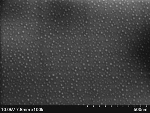
Figure 2 Surface SEM image of quantum dots
|
|
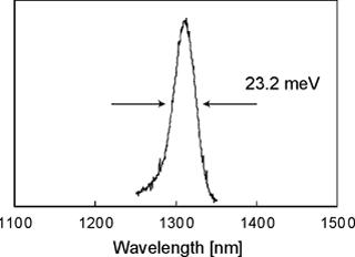
Figure 3 Emission spectrum of quantum dots
|
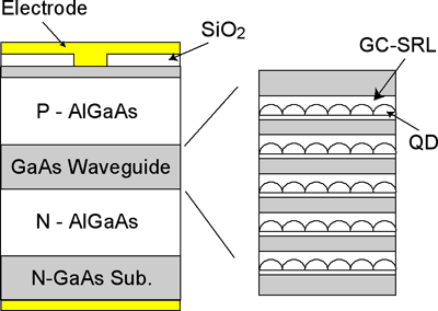
In this work, we have fabricated a quantum dot laser with five stacked layers of high density and uniformity dots as the active layer. The substrate structure consists of a GaAs layer for the waveguide layer, and an AlGaAs layer and conventional structure for the light confinement layer in addition to the active layer (Fig. 4). The laser waveguide takes a simplest gain waveguide structure to evaluate the performance of the active layer.
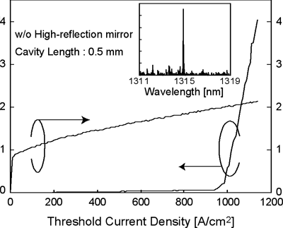
Unlike the conventional quantum dot lasers, our quantum dot laser without any high-reflection film mirror can oscillate at the 1.3 µm waveband even for a comparatively short cavity of 500 µm in length (Fig. 5). We evaluated its maximum modal gain, as shown in Figure 1, where the abscissa axis indicates a threshold current density for laser oscillation, and the ordinate axis indicates the modal gain. For comparison, a result for the laser with the three-stacked layers of the quantum dots is also shown, indicating that the modal gain saturates at 25 cm-1.
However, for five stacked layer, the modal gain showed a large value, 43 cm-1, without saturating. On the other hand, the values reported in other research institutes are, at most, 40 cm-1 even for 12 stacked layers, indicating that our quantum dot laser can attain a better modal gain characteristic in spite of the smaller layer number. This is caused by the success in producing the high density and high uniformity quantum dots.
 |
|
Figure 4 Cross sectional structure of quantum dot laser
|
 |
|
Figure 5 Oscillation characteristic and oscillation wavelength of quantum dot laser
|