What is Green, Sustainable Semiconductor Manufacturing Technology?
What is Green, Sustainable Semiconductor Manufacturing Technology?

2024/06/19

What is Green, Sustainable Semiconductor Manufacturing Technology?
The Real Reason Why Society is Paying Attention to Science

What is Green, Sustainable Semiconductor Manufacturing Technology?
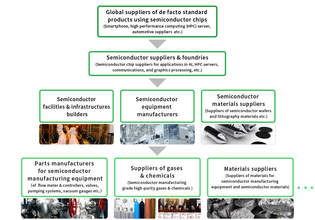
Green, sustainable semiconductor manufacturing technology optimizes all the input resources used in semiconductor manufacturing to minimize environmental impacts (greening), such as CO2 emissions, making semiconductor manufacturing more sustainable. Semiconductors are foundational products supporting a wide range of industries and are produced in large quantities. However, semiconductor manufacturing involves numerous processes, from raw materials to the final product, creating an exceptionally long supply chain. There are a wide variety of technologies and numerous companies involved, making it challenging to accurately assess the overall environmental impact of semiconductor manufacturing. It is urgently necessary to establish metrics to measure the current environmental impact and to develop countermeasure technologies based on these metrics to reduce the environmental burden.
Around 2020, the global semiconductor industry began taking action toward the greening and sustainability of semiconductor manufacturing technology. Semiconductor manufacturing is characterized by a long supply chain and involves a wide variety of related technologies and industries. To achieve a green and sustainable transformation across the entire semiconductor manufacturing process, individual company efforts are not sufficient; a collective industry-wide approach is essential. The National Institute of Advanced Industrial Science and Technology (AIST), as a public research institution, is actively working to lead in promoting these efforts. Since 2021, AIST has hosted the "Next-Generation Computing Infrastructure Strategy Conference," with one of its key goals being “the systematic development of green, sustainable semiconductor manufacturing technology.” The current status and details of green, sustainable semiconductor manufacturing—a topic now gaining significant momentum—are explained by Uchida Noriyuki, Director of the Research Planning Office of Electronics and Manufacturing.

The semiconductor manufacturing industry is steering toward green and sustainable practices
Semiconductors are now integrated into a wide range of products and are considered essential infrastructure for modern society. They serve as a source of industrial competitiveness and have a significant impact on economic security. Therefore, if sustainable production cannot be maintained, it could pose a significant risk to society. Meanwhile, amid concerns about climate change and resource depletion, all industries must adopt greener practices, such as reducing greenhouse gas emissions and minimizing resource consumption—and the semiconductor industry is no exception. To continue semiconductor manufacturing, green and sustainable practices are essential. This became widely recognized when Apple announced its goal in July 2020 to achieve 100% carbon neutrality across its entire supply chain by 2030. From this period, various initiatives began to emerge, including the Sustainable Semiconductor Technologies and Systems (SSTS) program by Imec, a semiconductor R&D hub in Europe, and the Semiconductor Climate Consortium (SCC) led by SEMI in the United States. AIST has also organized the "Green Sustainable Semiconductor Manufacturing Technology Study Group" as part of its activities in the Next-Generation Computing Infrastructure Strategy Conference, which examines future strategies.
What is necessary to advance sustainability efforts across the semiconductor industry?
The characteristics of semiconductor manufacturing include a long supply chain, a multi-stage production process, significant resource consumption, and the generation of large amounts of waste. For example, less than 1% of the input gas used in the semiconductor manufacturing process ends up in the semiconductor chip, with up to 99 % being discarded as waste. This means that only 1 % of the material is used in the final product, while the remaining 99 % is necessary for the process but ultimately discarded. Therefore, each stakeholder company is actively implementing measures focused on sustainability and green initiatives. By coordinating these efforts to ensure the entire group operates with a "common perspective," we believe the efficiency and effectiveness of these measures can be maximized. The activities of the SCC, led by U.S.-based SEMI, a major influencer in the global semiconductor industry, are also a key measure. AIST considers this "common perspective" a manufacturing metric for evaluating green sustainability and is advancing its development.
 Supply chain structure for green sustainable semiconductor manufacturing technology.
Aiming to establish metrics to be shared with all stakeholders
How can we create common metrics for green, sustainable semiconductor manufacturing? To address this challenge, a Green Sustainable Semiconductor Technology Study Group was established in 2022 within the Next-Generation Computing Infrastructure Strategy Conference. This group includes eight semiconductor manufacturing-related companies from Japan, as well as members from universities and research institutions, to discuss and explore future directions. The discussion defined the common metric as Green Manufacturing Metrics (GMM) and outlined the following policies.
1. Unified evaluation of all input resources as a third assessment metric for semiconductor manufacturing, alongside performance and cost
2. Development of concrete methods for calculating GMM
3. Standardization and dissemination of evaluation methods using GMM
4. Incorporation of a life-cycle assessment (LCA) approach to reduce environmental impact, reflecting actual conditions
The important concept is that these metrics are not intended for "regulation" but rather to provide feedback for the development of each technology.
What metrics is AIST considering for the GMM? To begin with, we are considering a model that converts all input resource quantities into carbon emissions (CO2 emissions). It is important that, as seen in Imec's SSTS program in Europe, the metrics for environmental impact are clear and easy to understand. Considering carbon pricing, we believe it is beneficial to convert resource usage into carbon emissions. Currently, various reports on carbon emissions associated with semiconductor manufacturing are being released. However, without publicly available information on how these emissions are calculated, it cannot be considered a "common perspective." Therefore, we believe it is necessary to develop calculation methods that incorporate the concept of LCA and to standardize these methods internationally. AIST has been selected for the Ministry of Economy, Trade, and Industry's international standardization survey project, starting in 2023, to promote the theme of "international standardization of green sustainable semiconductor manufacturing technology."
When constructing a model to calculate carbon emissions from semiconductor manufacturing based on LCA, a significant bottleneck arises. The bottleneck is the lack of carbon emission data for the production processes of semiconductor materials, such as gases, chemicals, and components. AIST is developing one of the world's largest LCA databases, called IDEA, which encompasses 18 areas and includes 5,300 datasets for evaluating the environmental impact of industries and formulating reduction measures.
Providing a formula as a guide for decision-making
We are developing a formula to calculate the environmental impact of semiconductor manufacturing while organizing carbon emissions data. It is a straightforward formula that converts all inputs used in the manufacturing process—including equipment (such as utility equipment and abatement systems), required utilities (like electricity and water), raw materials (such as silicon wafers and resins), gases, and chemicals—into carbon emissions and aggregates them.
The key point is that this formula enables each operator in the semiconductor supply chain to estimate the environmental impact of their products during the manufacturing process. By understanding the environmental impact of their products, companies can take measures such as developing products with lower environmental footprints to showcase the effectiveness of these efforts. It also assists semiconductor manufacturers in identifying which areas to prioritize for effectively reducing carbon emissions. Such formulas for calculating the environmental impact of semiconductor manufacturing need to be recognized globally. This initiative aims to establish internationally standardized metrics for green and sustainable semiconductor manufacturing.
Semiconductor manufacturing is divided into two main processes: the "wafer process," in which intricate circuits are etched onto the wafer, and the "packaging process," where the wafer is diced, encapsulated in resin, and formed into chips. We will develop a carbon emission calculation formula that reflects the characteristics of each process, allowing us to estimate the total emissions from the wafer to the chip. This necessitates collaboration with all businesses involved in the extensive supply chain. AIST aims to be the central hub for this collaboration.
In 2023, AIST established the Semiconductor Frontier Research Center (SFRC), which focuses not only on advanced semiconductor technology but also on developing technologies and GMM evaluation metrics aimed at promoting green sustainability. At SFRC, we have a research and development hub called the "Super Clean Room," which facilitates the processing of 300 mm silicon wafers and enables practical equipment process evaluations focused on green sustainability. Based on this center, we are establishing collaborative frameworks with in-house expert teams in environmental science, chemical processes, and other fields to address the diverse range of disciplines in green and sustainable semiconductor manufacturing.
In-depth discussions on green sustainable semiconductor technology are still in their early stages. However, centered around SFRC, we will fully leverage AIST’s strengths in collaborating with various government agencies, universities, and companies, both domestically and internationally, to advance the development and dissemination of green sustainable semiconductor technology for a better future.